Decoding Nvidia’s Blackwell Products: how do B200s, GB200s, HGX/DGX systems, and NVL supercomputers differ?
Introduction
One of the tricky things about Nvidia’s Blackwell architecture products is the easy conflation between chips, GPU-based systems, and supercomputers. For example, if you were to Google “Nvidia B200” you’ll find a mixture of posts detailing B200 GPU chips, Nvidia HGX B200s systems, and Nvidia DGX B200 systems. Despite sharing the same alphanumeric branding, these are three distinct products from three distinct product lines.
Today, we want to explicitly understand the difference between each of those product classes alongside Nvidia’s complete supercomputers. Additionally, we want to dissect the difference between B200s and GB200s which are often (and incorrectly) flattened into a single category. At a high level, here are the key differences:
- B200: GPU chips
- GB200: a superchip of 2 GPUs and 1 CPU
- HGX: multiple GPUs and interconnects system
- DGX: typically larger than HGX, sealed, plug-and-play system
- NVL: rack-scale supercomputer
As a forewarning, this article will be acronym-rich, filled with product names like HGX B200s, GB200 NVL72s, or DGX B300s tossed around. However, the conflating nature of these names is exactly why we want to clear up the confusion surrounding them.
To begin, let’s start with the basics: what is Blackwell Architecture?
What is Blackwell architecture?
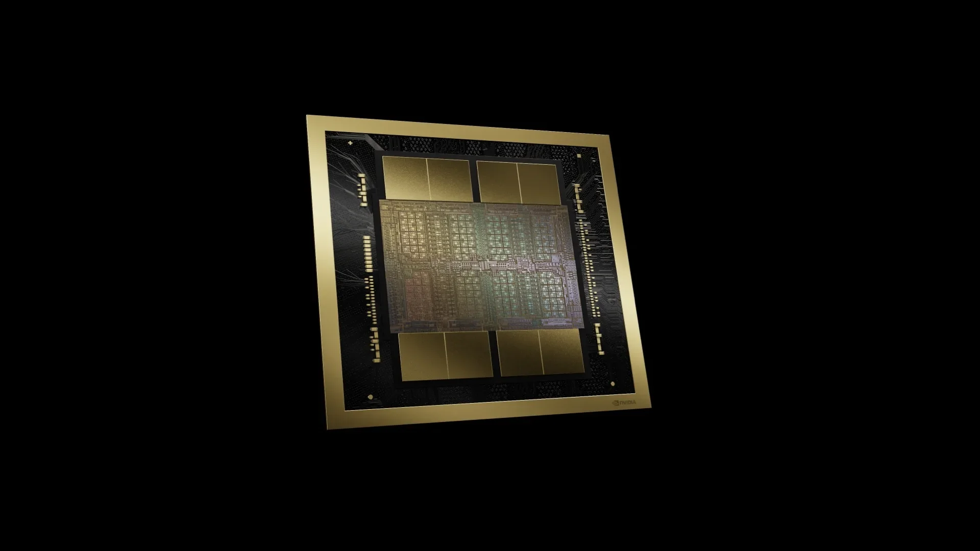
In 2024, Nvidia debuted their latest GPU series built on Blackwell architecture. Like the preceding Hopper architecture, Blackwell architecture was purpose-built for deep learning, now with even more specific hardware modules to mirror algorithm modules such as Mixture-of-Experts (MoE). But Blackwell architecture chips are also massive, with dual-die chiplets interconnected with a 10 Terabytes per second interior bridge.
Blackwell architecture chips have 208 billion transistors with 4nm precision manufactured by TSMC, considerably “spec’d up” from Hopper architecture which sported only 80B transistors. Blackwell chips also have significantly larger memory banks with 192 GB of HBM3e memory, up from 80 GB memory on Hopper Architecture.
What Blackwell architecture GPU chips are available?
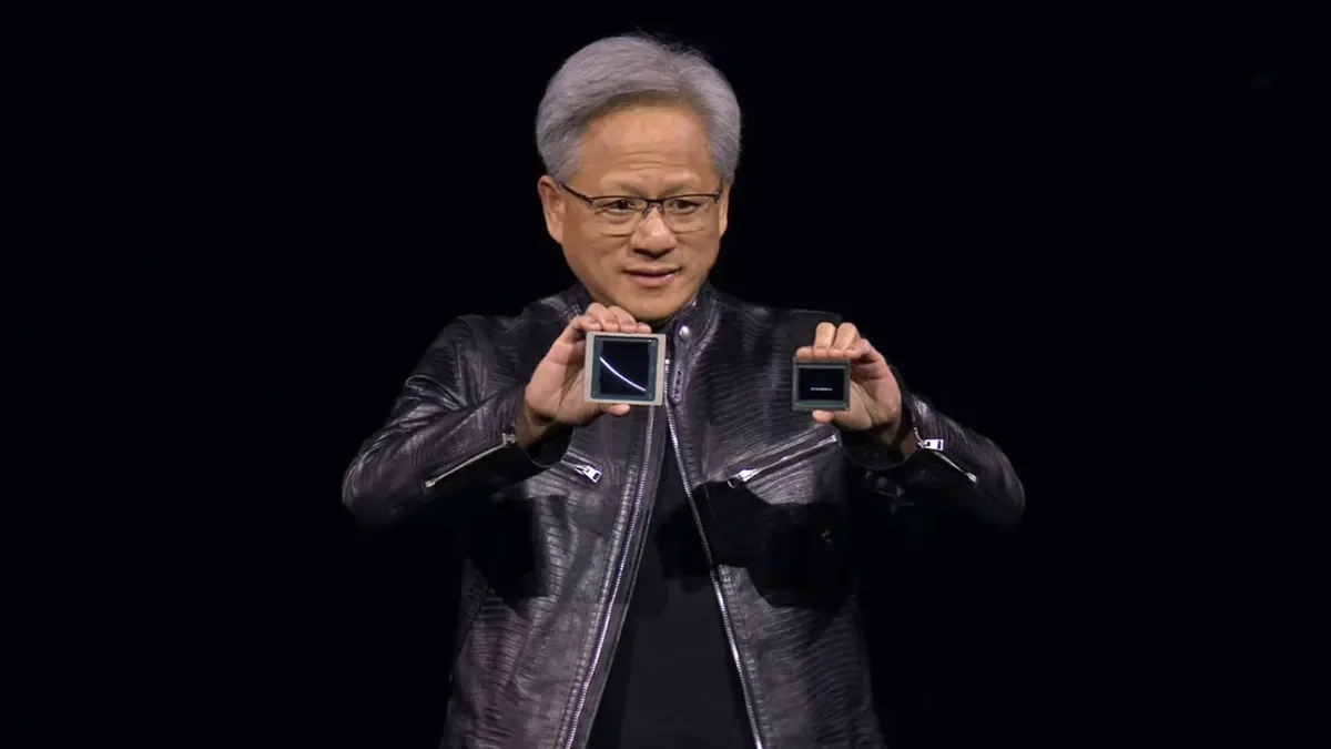
There are primarily three Blackwell architecture GPU chips: B100s, B200s, and the Blackwell Ultra chips.
B100s, B200s, and Blackwell Ultra chips are all dual-die with equivalent 208B transistor count. The B100s and B200s were released together, both with 192 GB of HBM3e memory (with 180 GB varieties), but differing power values of 700W TDP and 1,000W TDP respectively. The Blackwell Ultra, meanwhile, was a mid-cycle release with boosted architecture, supporting 288 GB of HBM3e memory and a maximum TDP of 1,400W.
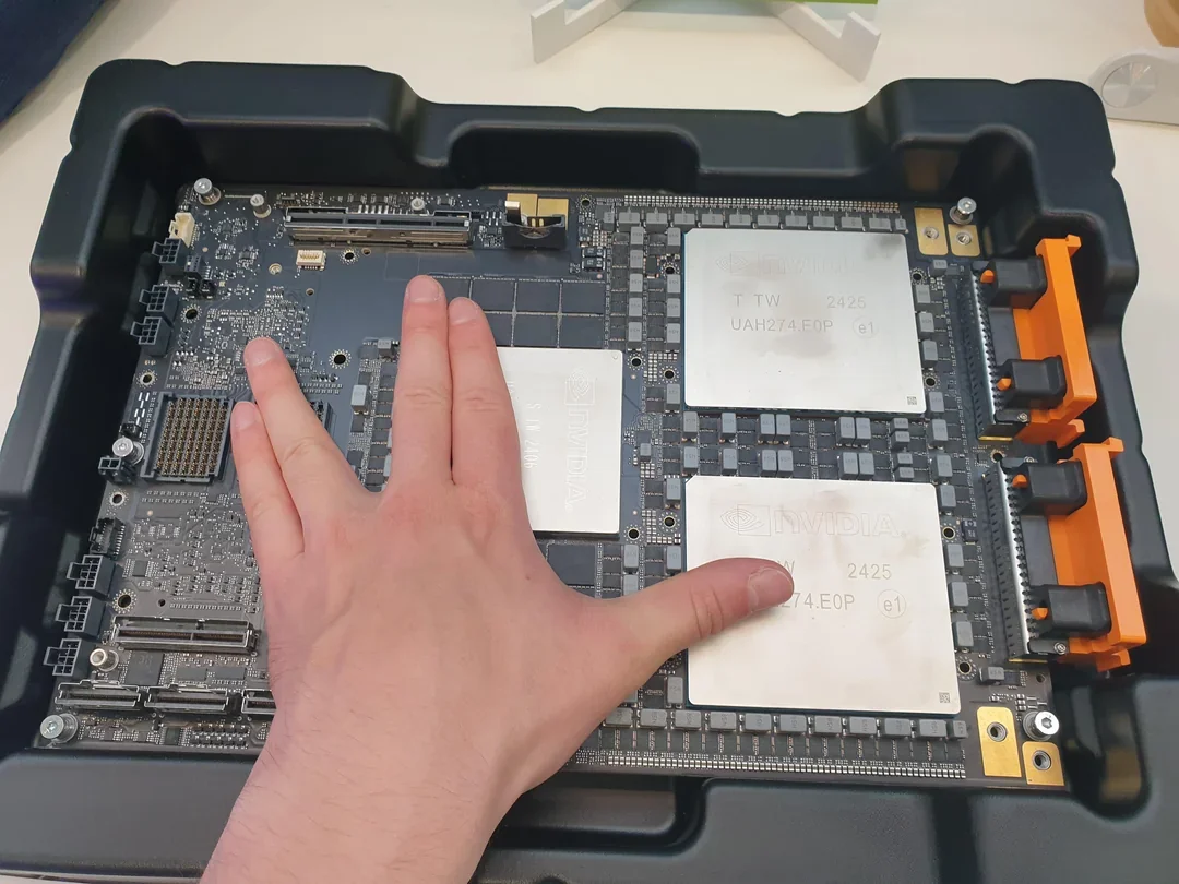
The Blackwell Ultra can easily be conflated with the GB200. Or, given they were announced at similar times, the GB200 might appear as the third option to the B100s and B200s. However, the GB200 is not a GPU, but a CPU-GPU superchip where 2 Blackwell GPUs are strewn together with 1 Grace CPU. In fact, the G and B of GB200 stands for Grace and Blackwell accordingly.
However, the GB200 is not available as a standalone product, but rather as 1 of 36 superchips in the GB200 NVL72 supercomputer that involves 72 Blackwell B200 GPUs and 36 Grace CPUs. There is also a recently announced GB300 NVL72, using the Blackwell Ultra GPU instead of the B200s. There also exist other configurations with just 16 and 8 superchips.
However, this is just the tip of the iceberg. At the end of the day, GB200s do share something in common with B100s, B200s, and Blackwell Ultras: they’re all considered chips, as opposed to platforms, systems, racks, or supercomputers. Those other words, rather, refer to Nvidia’s HGX, DGX, and NVL product lines.
GPUs vs HGX vs DGX vs NVL: what’s the difference?
The most confusing aspect about Nvidia’s product line is the difference between GPUs, GPU-based systems, and entire GPU-packed supercomputers. For instance, there colloquially is a B100, B200, and B300, but those aren’t exact corollaries (the B100 and B200 could refer to a chip, HGX unit, or DGX unit, but B300 is strictly a HGX or DGX unit). To clarify, this naming convention makes sense as it aligns the purpose of the product unit with the underlying hardware; however, to a hardware beginner, it could appear incredibly confusing.
Taking a step back, there are primarily four types of Nvidia products in the context of Blackwell architecture: GPUs, HGX platforms, DGX platforms, and NVL supercomputers (where systems and platforms for HGX and DGX are used interchangeably).
These are the aforementioned actual chips that chomp through numerical calculations to power deep learning or computations. Strict examples of these are B100s, B200s, and Blackwell Ultras. As a reminder, a GB200s are not a standalone GPU but a superchip of two Blackwell GPUs and a single Grace GPU.
Nvidia HGX Series
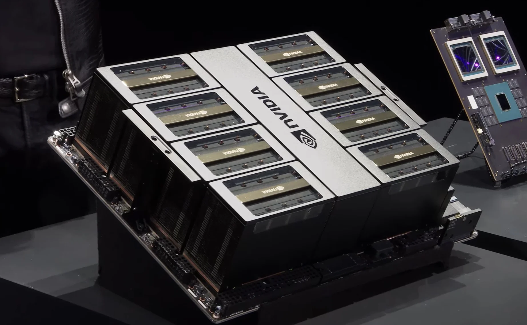
 HGX is a modular GPU-based system (often branded as a platform) that strings multiple GPUs and interconnects into a single unit that could be integrated with a larger computing system. These units are ideal for GPU vendors that want to configure their own GPU supercomputer. Some examples of Nvidia HGX units with Blackwell GPUs include the HGX B200 and HGX B300.
Nvidia DGX Series
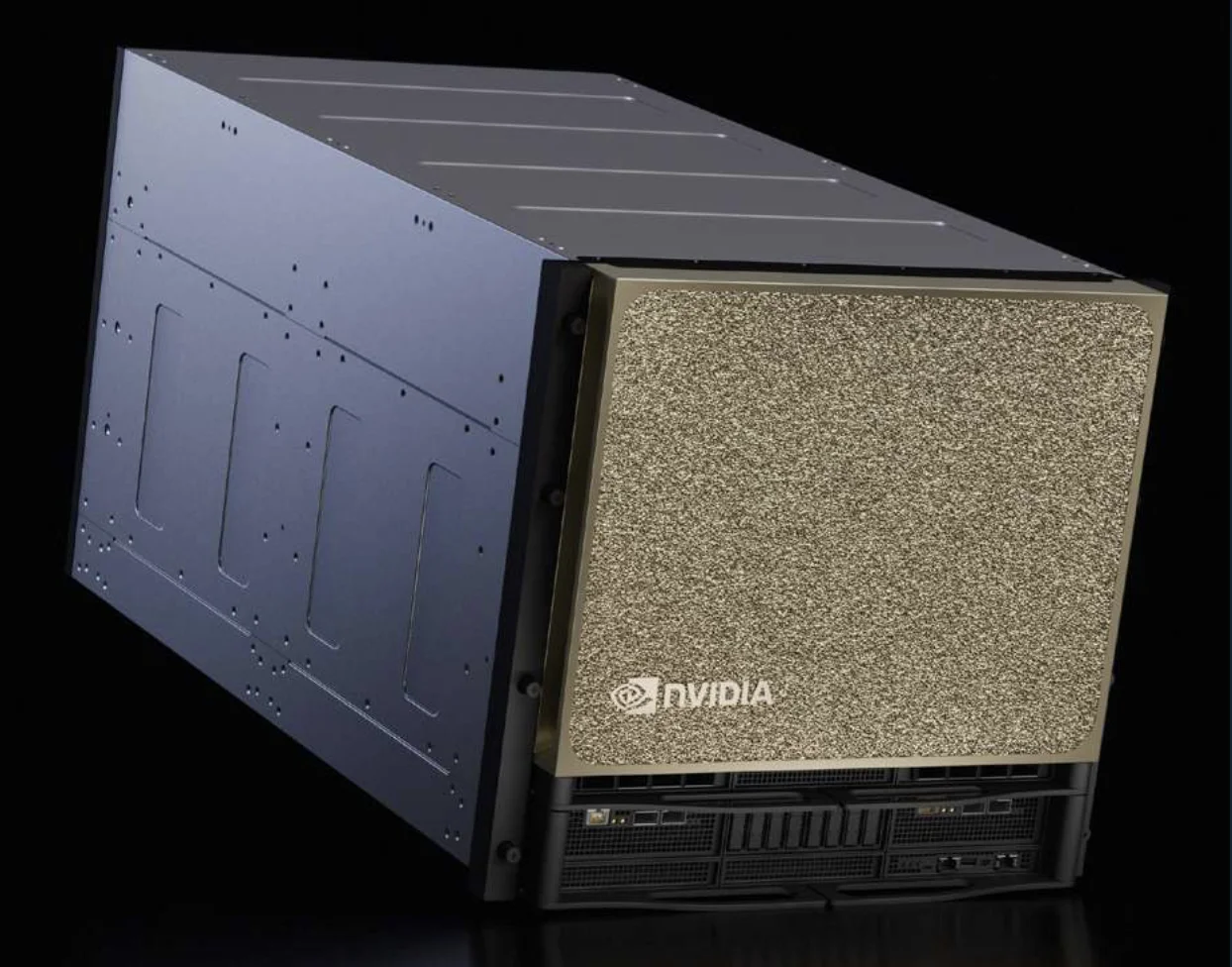
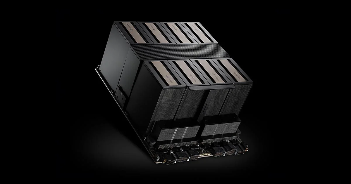
DGX are larger, blackbox GPU-based systems. While these can be parallelized to make an even bigger supercomputer (with Nvidia selling a pre-built solution known as DGX SuperPOD), the goal of a DGX is to provide a fully-functioning system that doesn’t require an additional scaffolding to be operational. However, each individual unit is not a supercomputer, at least by today’s standards. The one exception is the DGX GB200, a massive supercomputer capable of tackling trillion parameter models, made of multiple racks where each rack is the size of an Nvidia GB200 NVL72 (discussed in the next section).
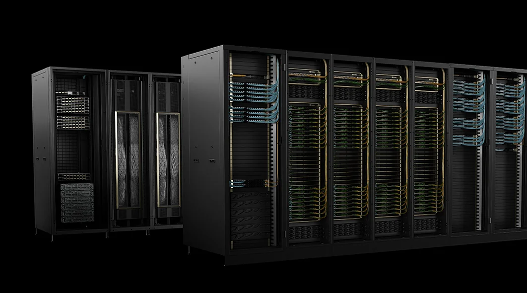
Nvidia NVL systems
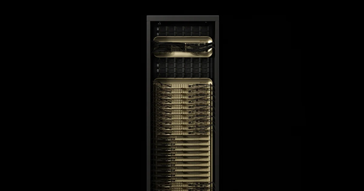
Nvidia also sells smaller units such as the HGX GB300 NVL16 and might likely release an even smaller unit to compare to the Hopper analog, the H200 NVL8.
The Hierarchy
Put crudely, GPUs < HGX < DGX ≤ NVL in terms of complexity and computing power. However, DGX computers are composed of GPUs, interconnects, and CPUs; at times, they are branded as involving multiple HGX units, however, that’s more of a matter of shared specifications than a direct encapsulation of units. NVL systems, meanwhile, strictly use Grace-Blackwell superchips (GB200 or GB300) instead of raw GPUs and CPUs that most DGX and HGX systems use.
That said, for a majority of developers, B100s, B200s, and Blackwell Ultras are the only relevant chips. Most are accessing these GPUs through GPU platforms (like Modal) and not directly purchasing baseboards or massive liquid-cooled supercomputers. In fact, most developers will strictly use the B200 GPU, the most available Blackwell GPU chip on the general market.
What is NVLink and NVLink Switch?
One of the cornerstone selling points of Blackwell architecture is it’s scalability where chips can be connected together to act as a bigger unit. This is made possible by NVLink and NVLink Switch that power high-speed, multi-GPU communication.
NVLink, now in its fifth generation, specifically lets GPUs share memory and computations for training and inference. Each Nvidia Blackwell GPU supports up to 18 NVLink connections where each connection supports 100 gigabytes per second (100 GB/s). Accordingly, a single chip can support up to 1.8 terabytes per second (1.8 TB/s).
NVLink Switch, meanwhile, makes it easy to leverage NVLink up to its full potential. NVLink Switch are independent chips that connect GPUs via NVLink within one or multiple racks! For example, the Nvidia GB300 NVL72 supports 130 TB/s of bandwidth by leverage 72 NVLinks orchestrated by an NVLink Switch. 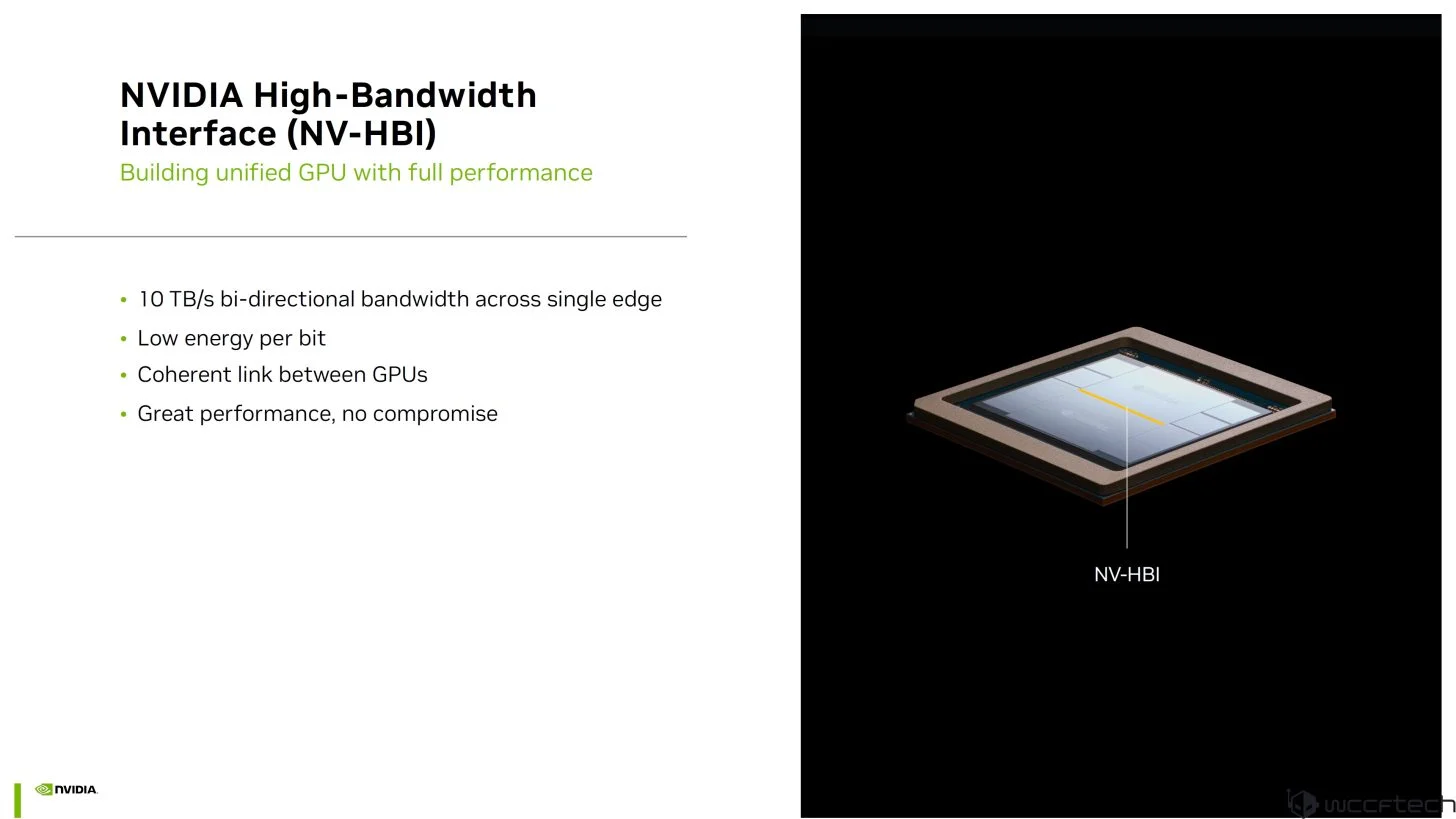
Closing Thought: The B200 is the most popular GPU
Many GPU providers skipped over the B100 and strictly decided to support the B200 (including Modal). There is a clear reason. Unlike Hopper Architecture, where the H100 and H200 had a different memory constraints, the B100 and B200 have an identical memory and, of course, architecture. The primary difference, however, is power consumption, where the B100 only supports up to 700W of power while the B200 can support 1 kW to 1.2 kW of power. This power differential leads to better efficiency on the B200 at scale, and for GPU vendors that are leasing out compute, that makes a no-brainer case to optimize for efficiency to minimize costs for the consumer.
If you want to train models or run compute jobs on B200s, sign-up for Modal today!